
The G5 is a 64-bit member of the PowerPC processor family that is fully compatible with 32-bit code. The second generation of G5 chips were first used in the Mid-2004 Power Mac G5. The design of these were massively updated with strained silicon, with a smaller fabrication size. These chips were also used in the iMac G5 iSight models.
The second G5 CPU, the PowerPC 970fx, was built on IBM taking its lessons from the first-generation 970, whilst simultaneously pushing towards the 3 GHz goal. The chip maxed out at 2.7 Ghz, still shipping as far along as Early 2005 Power Macs G5s. As a result, they fell short of their “GHz” goal, which is partly what prompted Apple to switch to Intel.
- See: IBM_PPC_970fx_G5-Gen2_Factsheet.PDF – (Download, 3.2 MB)
. - See: IBM970vs970fx.pdf.zip – (Download, 234 KB)
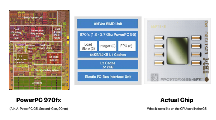
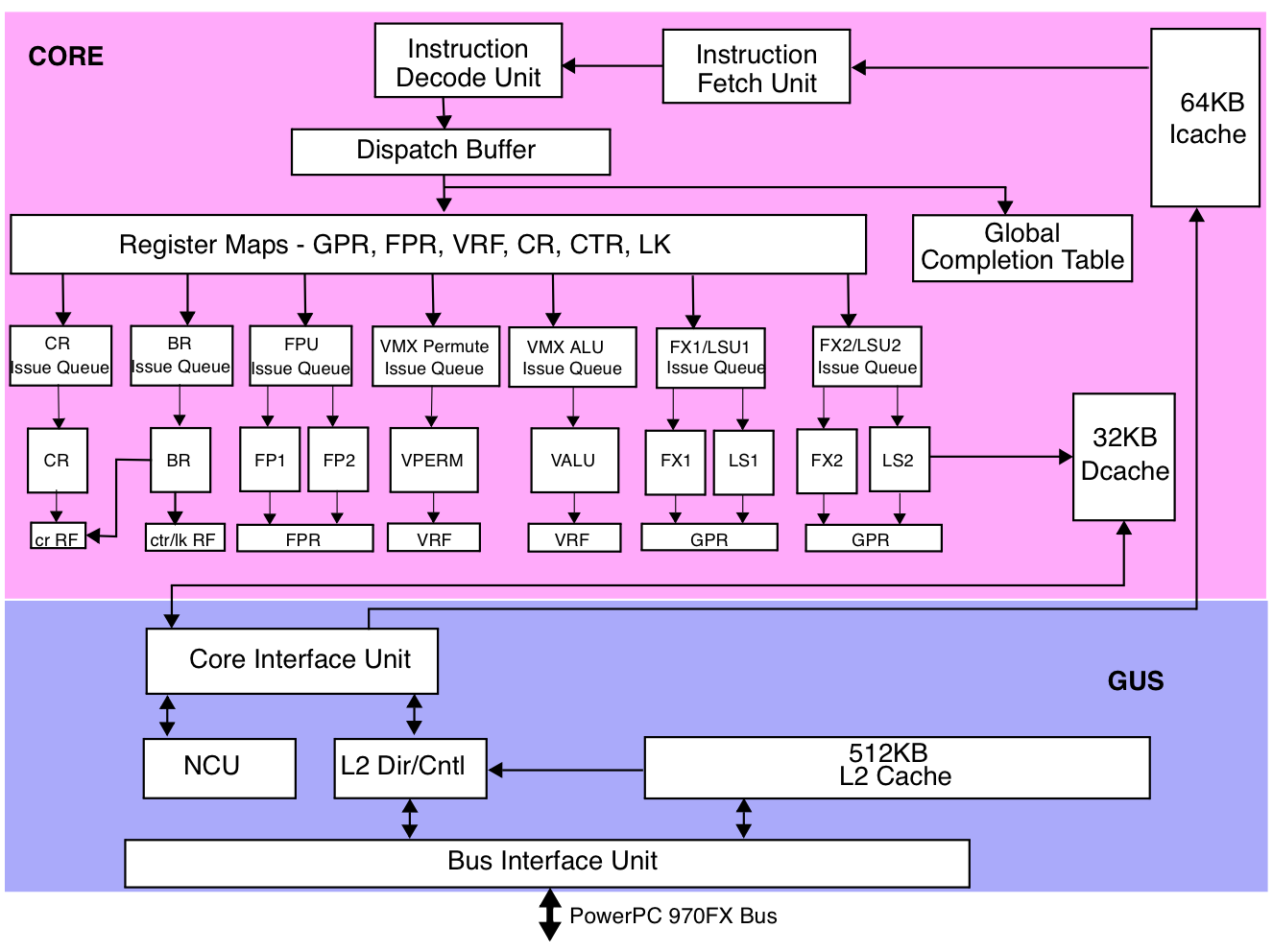
The 970fx shipped with 64 KB instruction cache and 32 KB data cache like all G5s – a step forward from using 32 KB for each throughout the G3 and G4 eras.
.
PowerPC 970fx Key Features and Notes
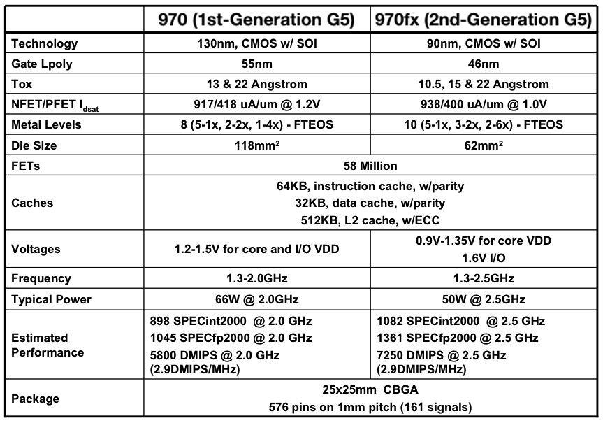
The main improvements of the second-generation G5 were the strained silicon, and smaller fabrication size. Strained silicon is a layer of silicon in which the silicon atoms are stretched beyond their normal interatomic distance.
.
 (Source: ISSCC 2004 / SESSION 3 / PROCESSORS / 3.7, CPU named edited by Mark)
.
90-nanometers is a massive step down from 130, which is a result mainly due to this new fabrication process. “Transistors made from strained silicon are said to get a 35 per cent performance boost over regular transistors of the same size.” says Tony smith of Personal Tech. When you add a layer of silicon over silicon germanium (SiGe), it results in a transformative process.
“The top layer’s silicon atoms align themselves with those in the SiGe layer’s wider-spaced crystal lattice, pulling them apart.” as it is mentioned in the Personal Tech article. IBM was using a different fabrication process at the time which aided the implementation of strained silicon called silicon-on-insulator (SOI).
Even though the G5 wasn’t able to get to the 3 GHz goal just yet, this was a massive leap forward in the right direction – this highlights precisely how the 2004 Power Mac G5s used less electricity versus the 2003 models. The 970fx uses far less energy versus the 970, and has the same amount of transistors.
.
How the G5’s System Bus works
To improve upon the G4 chips, the design also focused on a high-bandwidth memory bus which featured two unidirectional buses. On a 900 MHz System Bus, for example, the system is able to achieve up to a 6.4 GB/s useable bandwidth.
- Buses carry addresses and control signals in addition to data. You will see a % of peak bandwidth.
. - As the buses are unidirectional, each direction can realize only half the aggregate bandwidth.
. - This is the case for all G5 chips: The 970, 970fx, and the final 970MP.
.
Chip power draw
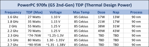
Official documentation states 35 Watts at 1.8 Ghz, which is what the 1.8 GHz PCI-X single-CPU Late 2004 Power Mac G5 has. IBM doesn’t have much (if any) official documentation past 2.2 GHz, so these are scaled estimates.
- Estimated based on voltage scaling and extrapolated from IBM’s provided figures for 1.6–2.2 GHz.
. - See More: Xserve G5 owner comments on CPU Power Usage/Heat (XLR8yourMac)
.
 .
.
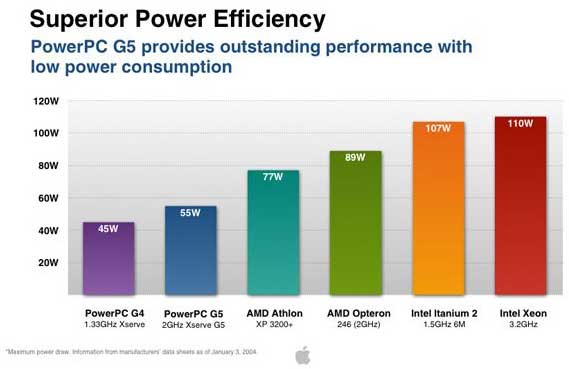
Compare to an original Mac Pro: Funnily enough, despite the amount of heat produced/complained about from the Power Mac G5, the second-gen IBM 970fx has nothing on the Clovertown Xeons from a 2007 Mac Pro (Only in terms of power draw).
- An Intel Xeon X5365 pulls 150 Watts at maximum, and an 8-core 2007 Mac Pro has two of them. Even so, there is a “PL2” maximum which allows this chip to push all the way to 206 Watts under the absolute heaviest of workloads.
. - Even a Dual 2.7 Ghz Power Mac G5 won’t pull as much electricity as a 2007 Mac Pro would. In fact, a base-spec Quad 2.0 2006 Mac Pro uses Intel Xeon X5130s, which use 10W more (65W versus 55W of a 2 GHz G5 970fx). Better performance-per-watt indeed.
.
 .
.
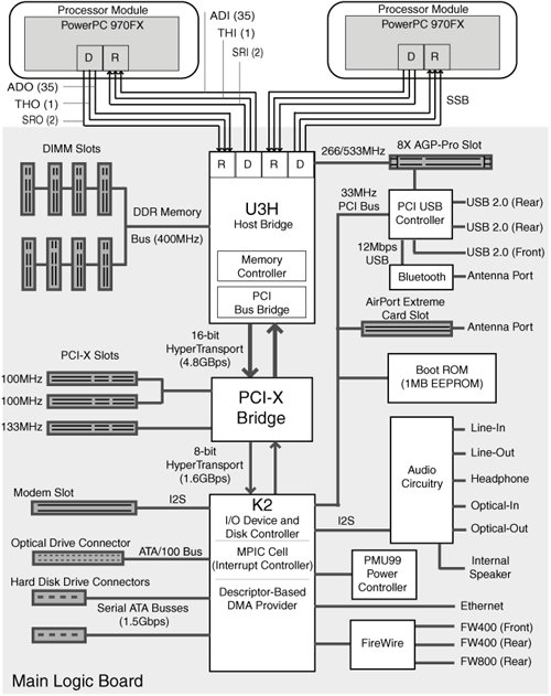
Mid-04 thru Early-05 Power Mac G5 Logic Boards
 .
.
Inside the PowerPC 970fx Second-Generation (Diagram)
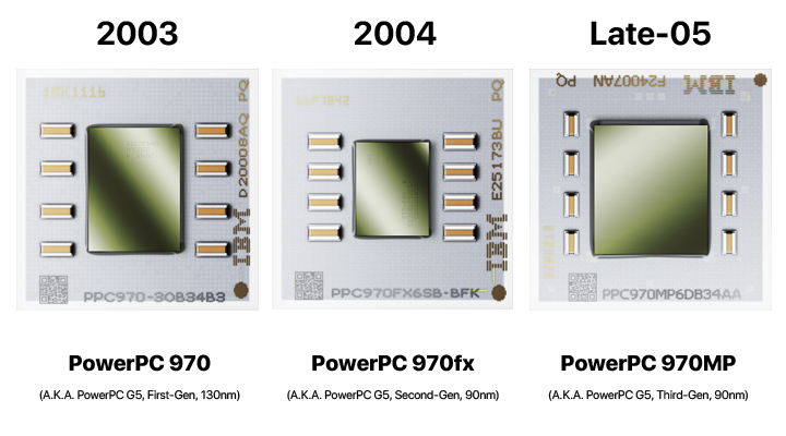
All three PowerPC G5 chips pictured
CPC925 Northbridge Chip
This is an Apple-designed chip made for the Power Mac G5, and used for the first and second generations of PowerPC G5 chips. It is also sometimes referred to as the Apple U3 or U3H (ECC variant) chip, capable of supporting up to two chips. There are two 550 Mhz unidirectional CPU buses, a 400 MHz DDR memory controller, 8x Pro AGP, and a 400 MHz 16-Bit HyperTransport tunnel.
An unfinished prototype version of this Northbridge chip exists called the U3L (U3Lite), which was made in development for the unreleased PowerBook G5. At lower clock speeds (like 1.5 GHz), it was becoming evident that a G5 was insubstantially faster than a similarly clocked G4.
Although the market had a strong demand for a better laptop CPU than the G4, the G5 and its Northbridge chip (even the prototype) just ate too much power. Even though the PowerPC 970fx was more power efficient than its 130nm 2003 predecessor, it lacked the power saving features needed in a ‘Book. For starters, they would simply eat way too much power when idling (both the G5 and NB chips).
.
Condensed CPU Specs
| Name: PowerPC 970fx
Released: Early to Mid 2004 Codename: PowerPC G5 (Second-Gen) Fabrication Process: 90-Nanometers Transistor Count: 52-58 Million CPU Family: Power4 Memory Data Path: 128-Bit Memory Type:.
~Bandwidth:.
Maximum RAM: 4 GB / 8 GB GPU Controller: AGP 8x Pro Mac Models: |
CPU Information:
Overall Cores:
L1i Cache: 64 KB per-cpu L1d Cache: 32 KB per-cpu L2 Cache: 512 KB per-cpu, ECC L3 or SLC Cache: None System Bus: 2:1
Total Power Draw:.
|