
Before Apple ever had their own custom in-house silicon with the debut of the A4 chip on the iPhone 4, there were Samsung chips. The first few iOS devices relied on these early chips, while every device since the first iPad sports a chip made by Apple. These are the known as the “A-Series” SOCs, which took on the naming convention from 2010 onward.
Fast forward to 2026, and the iPhone 17 lineup features the the ultra-powerful A19 and A19 Pro chips, which provide desktop-class Multicore processing, graphical power, and responsiveness out of a smartphone or a tablet. While the current lineup of mobile Apple SOCs may go toe to toe with chips like the M1 these days, the progress has been slow and steady over the years, incrementally building upon changes.
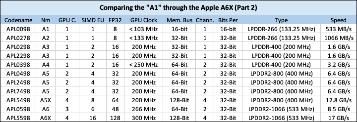
“APL0098” A.K.A. Apple A1 Chip
Known as the “APL0098” or Samsung S5L8900, this chip was used in the first-ever iPhone, iPod touch, and the iPhone 3G. The S5L89xx chips were adopted after the first prototypes of the iPhone used Freescale i.MX31 chips, and at the time they were designed more for power efficiency versus performance.
Also known as the ARM 8900B, it’s a 32-Bit ARMv6 chip with a 90-nanometer fabrication size, is under clocked to 412 MHz from the default 666 MHz, and features a whopping 16 Kilobytes of Level 1 Instruction cache as well as another 16 KB for L1 data. No L2 cache, no L3 or shared system cache – just one processor core, and a whopping 128 MB of 133.25 MHz of LPDDR-266, for a total memory bandwidth of 533 MB/s.
Fun facts:
- The fabrication size of a Samsung S5L8900 is also the same as an IBM PowerPC G5 Gen 2 – 90nm.
. - The RAM in a USB 2.0 iMac G4 runs faster than the RAM in a first-gen iPhone or iPod touch. (PC2700 333 MHz DDR vs LPDDR-266 133.25 MHz)
. - Devices: Original iPhone, First iPod touch, and iPhone 3G.
. - Announced: June 29th, 2007
“APL0278” A.K.A Apple A2 Chip
There’s no such thing as an “Apple A2” chip, but it’s a very fitting name considering it was only ever used for the second generation iPod touch. It’s very similar to the Apple A1 S5L8900, except it’s a 65nm chip instead of a 90nm one, with some other differences as well.
- A slightly higher cpu clock: Bumped to 533 MHz over the original 412 MHz
. - Also a slightly higher GPU clock: 103 – 133 MHz dynamically adjusted GPU clock with 1.64 – 2.12 GFLops of performance.
. - Announced: July 11th, 2008
“S5L8920/S5L8922” A.K.A. The Apple A3
The S5L8920 was used in the iPhone 3GS, whereas the S5L8922 is a variant used in the 3rd-generation iPod touch. One of the key differences which separate the A3 series from the A1/A2 is the doubling of both L1 Instruction and data caches, increasing to 32 KB per-core, thus, contributing to the improved performance.
Memory bandwidth is doubled to 1.6 GB/s, now featuring 256 MB of LPDDR-400 (200 MHz) for more performance improvements over previous generations. The maximum GPU clock has also been increased to 200 MHz, and this chip finally also adds sorely needed 256 KB of L2 cache. Prior to the 3Gs, there was literally no L2 cache in any device running iOS.
Fun Fact:
- While the iPhone 3GS SOC has a 65nm fabrication size, the iPod touch 3G’s S5L8922 is a 45nm variant of the same chip. This also means it has a smaller die size – (36 mm2 vs 72 mm2)
. - First Announced: June 19th, 2009
- For iPod touch 2nd Gen: September 9th, 2009
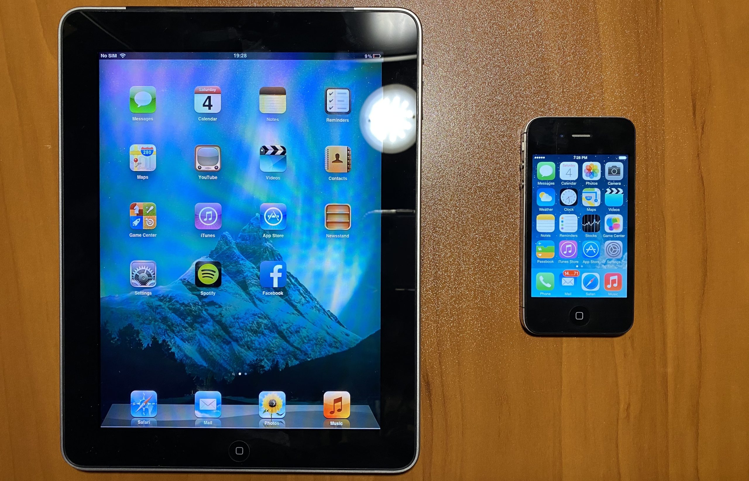
The A4 chip
 Now THIS is actually the very first Apple Silicon chip designed in-house, much like the Apple Silicon M series we grew to love. It was still 32-bit, powered the iPhone 4, original iPad, and the 4th-generation iPod touch.
Doubling-down over the previous generation’s L2 Cache, the A4 brings it to 512 KB. CPU clock speeds are incrementally bumped up as well, going up to 800 MHz – 1 GHz depending on the device. Memory bandwidth has also increased to 3.2 GB/s for all devices on this SOC.
Fun facts:
- If you’re on an OG iPad or Apple TV only: It’ll go up to 1 GHz. The iPhone 4, and 4th-Gen iPod touch go up to 800 MHz.
. - This chip was also used in the second-generation Apple TV.
. - There’s no RAM on the SOC. It’s connected to the processor using the 64-Bit wide ARM AMBA 3 AXI bus. Just like the iPhone 3GS, any Apple device with an A4 uses LPDDR-400 (200 MHz), and the memory chips often (or always) come in pairs.
. - Announced: April 3rd, 2010
All the different A5 chips
Technically there are four different A5 chips if you count the A5X – including a locked-down 1-core version made specifically for the 3rd generation Apple TV (Wait, I thought all A5s were Dual-Core)? All A5s feature improved L2 cache over A4s, faster memory, and a faster graphics core.
Released alongside the 2nd Generation iPad in March 2011, Apple touted the A5 as “can do twice the work” versus the A4, as well as 9x graphical performance. All A5 and A5X chips feature 1 MB L2.
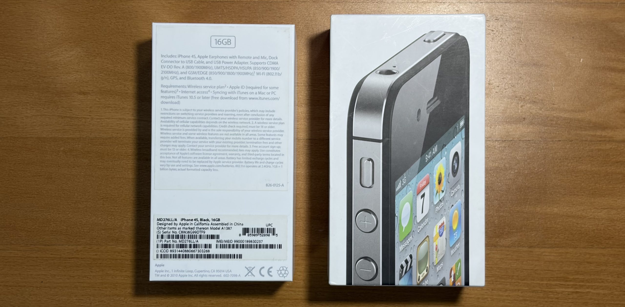
- APL0498 45nm – Released March 11th, 2011, featured in the iPhone 4s and iPad 2,1
. - APL2498 32nm – Original iPad mini, iPad 2,4, iPod touch 5th Generation
. - APL7498 32nm – Apple TV 3rd Generation (one core locked)
. - (A5X) APL5498 45nm – iPad 3rd Generation
Then there was the 3rd generation iPad, which shipped alongside an A5X – a higher power version of the A5. Featuring a quad-core graphics chip, it improves graphical performance to 25.6 Gigaflops, and makes a number of technical improvements over the A5.
- Memory Bandwidth is doubled to 12.8 GB/s over 6.4 GB/s
. - Memory Bus Width is double, at 128-Bits wide versus 64-Bits.
. - First Announced: March 11th, 2011
- Again for: iPod Touch Gen 5, Apple TV Gen 3, OG iPad mini + iPad2,4 – March 7th, 2012
- Apple TV 1-core version: January 28th, 2013
- 5th-Gen iPad version: March 16th, 2012
The A6 and A6X
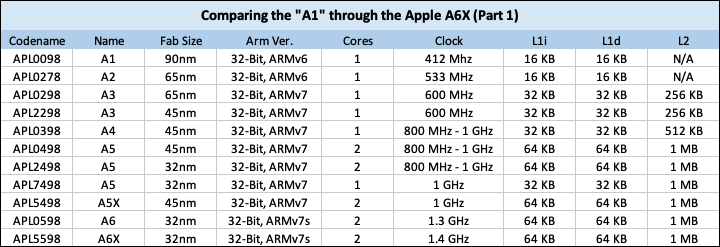
Finally the chips are creeping over that 1 GHz CPU clock speed threshold, seeing 1.3 GHz in the iPhone 5/5c, and 1.4 GHz in the 4th Generation iPad with an A6X. The type of RAM is also upgraded over the A5 series, now using LPDDR2-1066 (533 MHz) at 8.5 GB/s memory bandwidth, and 17 GB/s for the iPad 4th-gen. GPU clock is also slightly higher on the 4th-Gen iPad, at 300 MHz vs 266 MHz on the iPhone 5/5c.
- A6 Announced: iPhone 5, iPhone 5c – September 21st, 2012
- A6X: iPad (4th Generation) – November 2nd, 2012
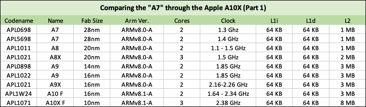
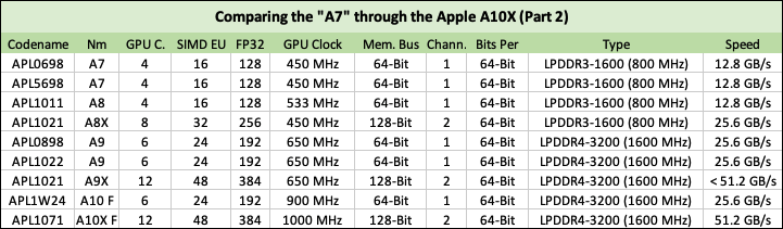
Apple A7: Kicking it up a notch
Introduced September 10th 2013 alongside the iPhone 5s as the first 64-Bit Mobile Apple Silicon, the Apple A7 also saw use in the second-Gen and third generations of iPad mini, as well as the OG iPad Air. Featuring a Billion transistors and an even smaller fabrication size, the A7 makes a number of improvements over the outgoing chip.
- First Apple-Designed SOC to feature any L3 cache, 4 MB Inclusive. Prior Apple SOCs had none.
. - L1i & L1d are both doubled to 64 KiloBytes Per-Core, totaling for 128 KB L1.
. - These are the first Apple mobile devices to adopt DDR3 of any form, using 800 MHz LPDDR3-1600 running at 12.8 GB/s.
. - Fabrication: 28nm High-K dielectric metal gate
. - 1.3 GHz APL0698: iPad mini (2nd and 3rd Gen), iPhone 5S
. - 1.4 GHz APL5698: OG iPad Air
. - First Announced: September 20th, 2013
- For OG iPad Air: November 1st, 2013
iPhone 6, 6 Plus, and the Apple A8
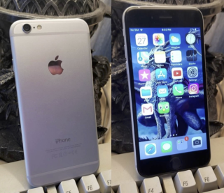 Apple finally heard the call of people – “Give us a bigger iPhone!” ..and so they did! The iPhone 6 and 6 Plus were by far the most popular iPhones ever, with about a quarter of a billion devices sold worldwide – also making them the most popular smartphone, to-date.
Editor’s Note: This was my iPhone 6 when I still had a Samsung Galaxy S8+ from Sprint, to test and try out how much iOS had evolved since I stopped using the iPhone 3GS in 2012. Enough had changed by then since I last used iOS, and this experience eventually led me to buying an iPhone X.
Fun facts:
- The A8 doubles transistor count to 2 Billion, (3 Billion for A8X), up from 1B for the A7.
. - An Apple A8 also uses the 20nm fab size, w/High-K dielectric metal gate.
. - Uses the same RAM as the Apple A7 chip: LPDDR3-1600 (800 MHz) @12.8GB/s
. - Clock speeds can now reach up to 1.5 Ghz, but tend to stay a lower clock speed on an iPhone versus an iPad.
. - Believe it or not: This had one of the longest production runs of any Apple SOC ever – Beginning September 9th 2014, surviving all the through to October 18th 2022, the same date the much newer A12 was discontinued. (Source: https://en.wikipedia.org/wiki/Apple_A8 – 2/28/26)
. - Announced: September 19th, 2014
- For iPad Air 2: October 22nd, 2014
Apple A9, A9X, and a new manufacturer – TSMC
There are two nearly identical versions of the A9 chip – one made by Samsung which went into the 6s, 6s Plus, and a later TSMC version which went into the iPhone SE. It’s also the first Apple device to use any iteration of DDR4, beating Macs by about 2 years, which didn’t see DDR4 until the 2017 5K iMac.
Featuring a brand-new custom storage solution, the A9 chip sports an Apple-designed NVMe controller, introducing PCI Express, and much faster storage for the iPhone 6s and beyond. This is right when internal storage started getting much faster on iPhone.
Major improvements:
- 14nm and 16nm fabrication sizes
. - Clock speeds reach up to 1.85 GHz, and up to 2.26 GHz on the A9X with the first-gen iPad Pros.
. - Memory speed and and bandwidth is improved: LPDDR4-3200 (1600 MHz), @25.6 GB/s
. - GPU clock is also improved, increasing to 650 MHz w/249.6 GFLops of performance. This is a drastic leap forward over the even more powerful iPad A8X, which only did 230.4 GFLops.
. - Announced: September 9th, 2015 (Samsung & TSMC versions)
- A9X: For iPad Pro Gen 1 – November 11th, 2015
iPhone 7, The A10 Fusion, A10X Fusion, and T2 Chip
With the release of the iPhone 7 and 7 Plus on September 16th 2016, we finally got the A10 Fusion along with something we take for granted these days without even realizing it: Efficiency Cores. The A10 Fusion was the first-ever Quad-Core Apple SOC, packing 40% better CPU performance and 50% more GPU performance over the A9, according to Apple.

- First to implement ARM’s big.LITTLE fab design – Powerful/hungry cores + small/efficient cores inside a single chip package for better battery saving versus clock scaling alone. In benchmarks, the A10 shows up as a dual core chip, however. This is because unlike other chips which use the big.LITTLE implementation, the A10 Fusion can only use either it’s efficiency cores or it’s performance cores.. but not both at the same time.
- Remember that T2 security chip from the late Intel era? It’s a heavily modified A10 Fusion, serving as a security coprocessor for certain models. The T2 is a bit unusual versus it’s derivative:
.- If your Mac was purchased with 1 TB SSD storage or more, your T2 chip will have 2 GB LPDDR4-3200, or only 1 GB LPDDR4 is the Mac shipped with < 1 TB storage.
. - The T2 is a full-on Quad-Core SOC with yet another 32-bit ARMv7-A Secure Enclave Processor (SEP) secretly stuffed inside, to handle encryption keys. This hidden gem also runs its own OS underneath even the bridgeOS, called sepOS. It’s an OS within an OS, within an OS (sepOS > bridgeOS > macOS).
- A T2 security chip communicates with the Mac via a USB-attached ethernet port.
- If your Mac was purchased with 1 TB SSD storage or more, your T2 chip will have 2 GB LPDDR4-3200, or only 1 GB LPDDR4 is the Mac shipped with < 1 TB storage.
- Announced: September 16th, 2016
- A10X Fusion: for iPad Pro Gen 2 + Apple TV 4K (2017) – June 13th, 2017
Source for information used in this article: (Wikipedia, the free encyclopedia, https://en.wikipedia.org/wiki/Apple_silicon, Saturday, February 28th 2026 1:53 EST, URL)
